
- Reaction score
- 12,964
- Points
- 1,160
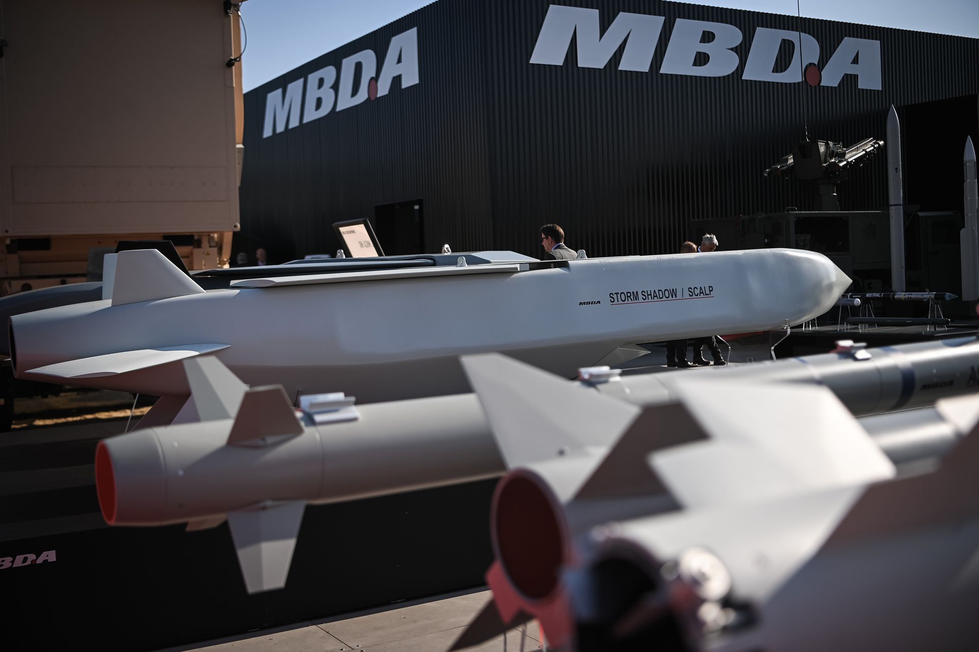
Ukraine used Storm Shadow to strike Russia's most irreplaceable weapons factory — and why it matters
As you read this, somewhere at a TSMC fab in Taiwan's Hsinchu a robot is moving a silicon wafer packed with transistors measuring 2 nanometers — 20 atoms in a row. Mass production of chips using the 2-nanometer process began in late 2025, and TSMC's entire 2026 capacity is already sold out —...
 kyivindependent.com
The article headline is a Storm Shadow attack.
Here are the really important bits.
2 nanometers
"As you read this, somewhere at a TSMC fab in Taiwan's Hsinchu a robot is moving a silicon wafer packed with transistors measuring 2 nanometers — 20 atoms in a row.
1.8 nanometers (Edit: 10% increase in efficiency)
"Mass production of chips using the 2-nanometer process began in late 2025, and TSMC's entire 2026 capacity is already sold out — Apple, Qualcomm, NVIDIA, and AMD are all in line. Samsung has launched its own 2-nanometer Exynos 2600 processor. Intel is advancing its 18A node (1.8 nm)."
90 nanometers
Now — Russia. Its most advanced serial (not experimental) process is 90 nanometers at the Mikron plant in Zelenograd, a city near Moscow. That is the level TSMC reached in 2004.
250 to 350 nanometers
The Kremniy El plant in Bryansk — until recently Russia's second-largest producer of microelectronics for the Defense Ministry — was serially manufacturing products at 500 nm design rules, had theoretical capabilities in the 250–90 nm range, and was planning to reach serial 350 nm production for more complex devices.
500 nanometers
For comparison: 500 nm is mid-1990s by global standards.
.....
Mass is a function of volume and volume is the cubic function of length.
If a given number of transistors are required to achieve a specific function then they occupy a specific volume and have a specific mass. That volume and mass require a specific size of vehicle and a specific amount of energy to move it.
If L = 500 and V is L cubed then V = 500 x 500 x 500 or 125,000,000 units and mass will follow accordingly.
If L = 2 the V = 2 x 2 x 2 or 8 units. And mass will follow accordingly.
125,000,000 nm3
8 nm3
We are getting into the realms of angels and pins.
....
But...
A cruise missile does not need a processor capable of running large language models that it would chat with before diving into a thermal power plant near Kyiv.
It needs a reliable, vibration- and temperature-resistant microchip that correctly processes guidance system signals. Power electronics, discrete semiconductors, and analog microchips — none of this requires cutting-edge lithographic processes, but all of it requires specialized manufacturing. That is exactly what Kremniy El was making.
....
What is possible.
What suffices.
....
What constitutes a critical supply node?
